In advanced machine vision, medical devices, automotive ADAS, and high-speed robotics, off-the-shelf processing units often struggle with real-time video capture and ultra-low latency demands. This is where an FPGA Hardware Integrator becomes critical.
An FPGA Hardware Integrator specializes in developing customized hardware architecture, custom PCB layouts, logic IP cores, and low-level drivers to create tailored, high-performance “hardware brains” for complex computing applications.
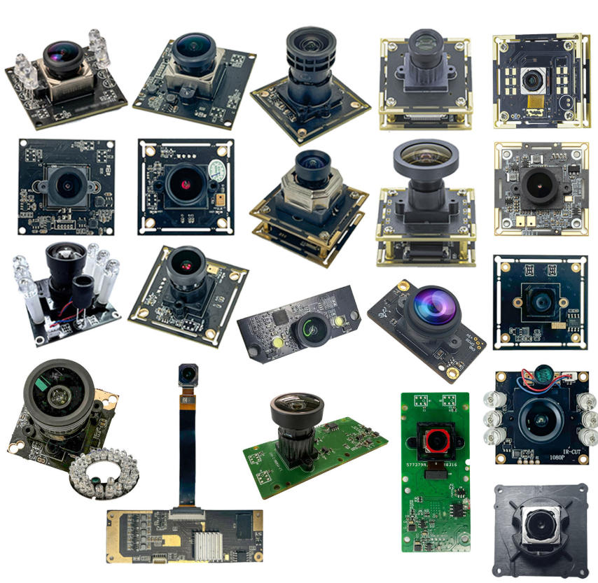
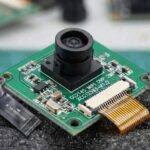
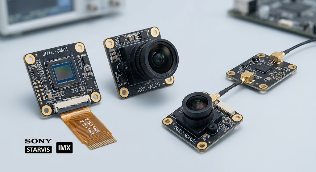
At Joyllon, we collaborate directly with engineering teams and system builders to deliver high-precision board-level camera modules, custom MIPI/LVDS sensor heads, and flexible OEM/ODM imaging solutions designed specifically for FPGA hardware integration.
What is an FPGA, and Why Do You Need a Hardware Integrator?
An FPGA (Field-Programmable Gate Array) is a semiconductor chip with an internal circuit structure that can be reconfigured and reprogrammed repeatedly via code. Unlike CPUs or GPUs—whose hardware architecture is permanently fixed after manufacturing—FPGAs allow logic gates to be wired digitally on the fly.
The Engineering Challenge
While FPGAs offer ultra-fast parallel processing speeds and microsecond-level latency, developing custom FPGA hardware from scratch requires deep expertise in digital circuit design using HDL (Hardware Description Languages like Verilog or VHDL). Most equipment manufacturers (e.g., medical endoscopy, drone avionics, industrial inspection) lack the internal bandwidth or specialized personnel to build custom high-speed FPGA boards and register-level firmware.
The Role of the Integrator
An FPGA Hardware Integrator bridges this engineering gap. They select raw FPGA silicon, design multi-layer high-speed PCBs, optimize high-speed camera interfaces (such as MIPI CSI-2, Sub-LVDS, and PCIe), write custom logic code, and solidify algorithms—delivering a plug-and-play hardware engine ready for deployment.
Core Capabilities of an FPGA Hardware Integrator
Delivering custom FPGA hardware solutions requires a fusion of high-frequency PCB engineering, RTL firmware development, and driver adaptation:
1. High-Density PCB & Board-Level Design
- High-Speed Layouts: Engineering 10-to-20+ layer PCBs designed to overcome Signal Integrity (SI), Power Integrity (PI), and thermal dissipation challenges.
- Versatile Interface Integration: Integrating high-bandwidth camera and communication protocols including MIPI CSI-2, Sub-LVDS, LVDS, GMSL/FPD-Link, PCIe, and 10G Ethernet/SFP+.
2. Logic & IP Core Development
- Hardware Accelerators: Writing RTL code to execute hardware-level image processing, including real-time noise reduction, distortion correction, and edge detection.
- Protocol Bridging: Converting raw camera module feeds (MIPI or LVDS streams) directly into standard interfaces like HDMI, USB 3.0, or PCIe with near-zero latency.
3. Firmware & Driver Integration
- System Co-Design: Developing Linux and Windows device drivers alongside SDKs to enable smooth communication between the FPGA board and host carrier processors.
Applications in Machine Vision and Embedded Cameras
FPGA integration plays a transformative role in vision processing and multi-camera systems:
- Ultra-Low Latency Multi-Camera Synchronization: While traditional CPUs suffer frame drops and latency when ingesting multiple 4K video feeds, FPGAs achieve nanosecond-level, parallel video frame synchronization.
- Custom ISP & Raw Video Processing: Raw image data (Raw RGB/YUV) output from custom camera modules can be piped directly into the FPGA for real-time ISP tuning, hardware compression, or stream conversion before transmission over GMSL or optical fiber.
- Miniaturized High-Density Hardware: For ultra-compact systems like laparoscopic surgical devices or industrial inspection heads, FPGA integrators condense the sensor interface, processing logic, and output bus onto a single compact PCB assembly.
Partner with Joyllon for Custom FPGA Camera Module Solutions
FPGA hardware integrators are essential technology facilitators connecting silicon manufacturers to end-user equipment builders. To maximize the performance of an FPGA-based vision engine, pairing it with high-precision, low-latency camera hardware is paramount.
At Joyllon, we support FPGA engineers with:
- MIPI CSI-2 & Sub-LVDS Camera Modules: Native high-speed board-level modules optimized for FPGA interface connectivity.
- Active Alignment (AA) Manufacturing: Cleanroom lens assembly guaranteeing maximum optical centration and corner-to-corner clarity.
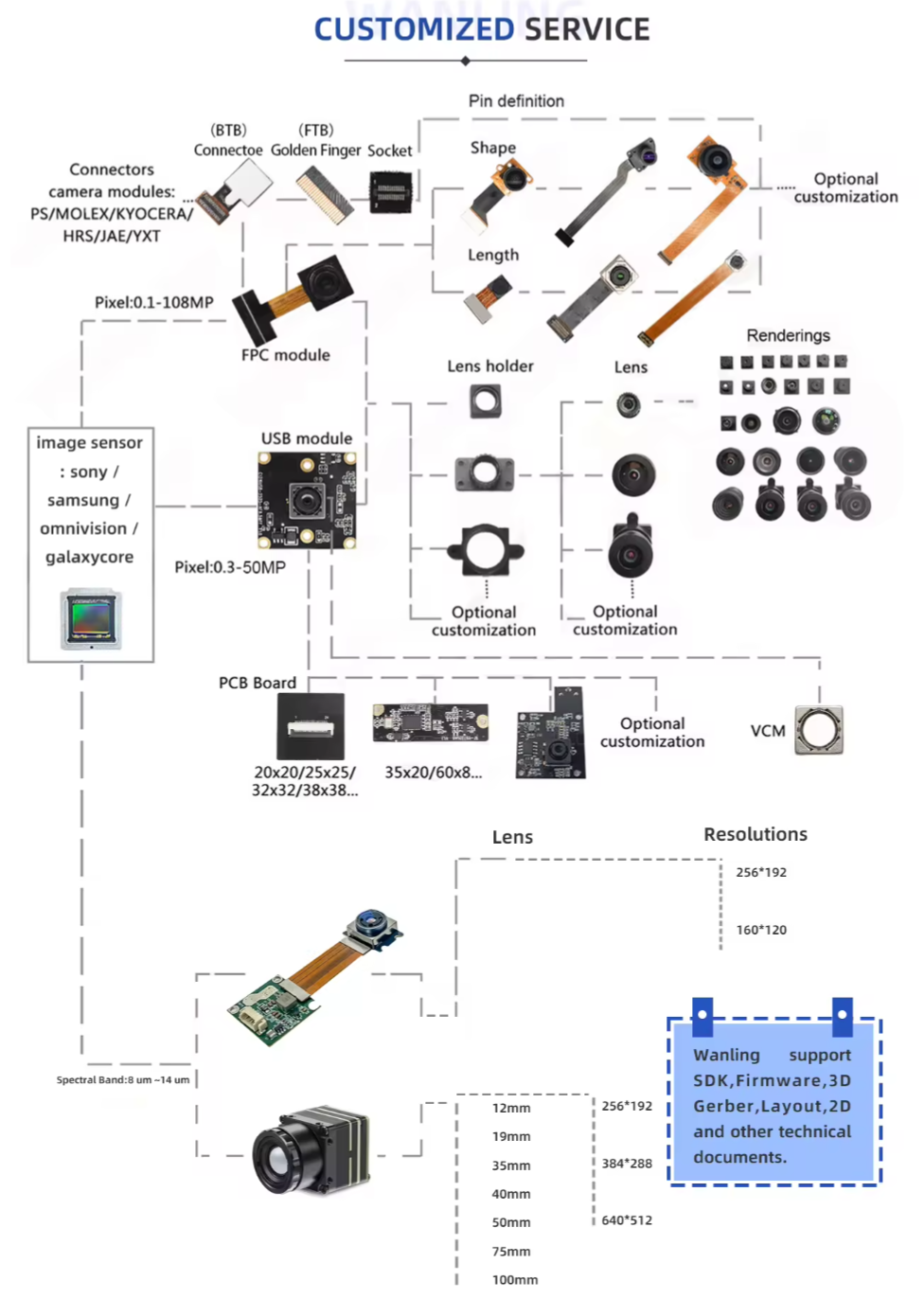
- Flexible OEM/ODM Customization: Custom PCB shapes, flexible flat cables (FFC), and sensor pinout matching tailored to your FPGA carrier board requirements.
Learn more about our custom camera module design and manufacturing capabilities at www.joyllon.com or reach out to our engineering team to discuss your next embedded vision project.
📞 Contact US now!
- - Need a Prototype or Datasheet?
- Get Real Testing Videos?
- Request a Product Catalog & Price List? (Low MOQ / OEM/ODM / Sample supported? - 🌐 Official Website: www.joyllon.com
- 💬 Tel: +86 137 1379 2667 ( only email, it is formal)
- ✉️ Corporate Email: b2b@joyllon.com and chinaok321@gmail.com (Get a Free Quote within 24 Hours)
👉or fill in below form, we will answer you within 24Hrs.